The Main Memory System
Main memory is a critical component of all computing systems: server, mobile, embedded, desktop, sensor
Main memory system must scale (in size, technology, efficiency, cost, and management algorithms) to match the growing demands of bandwidths
Memory System: A Shared Resource View
Memory System: A Shared Resource View State of the Main Memory System
Recent technology, architecture, and application trends
exacerbate old requirements
DRAM and memory controllers, as we know them today, are (will be) unlikely to satisfy all requirements
Some emerging non-volatile memory technologies (e.g., PCM) enable new opportunities: memory + storage merging
We need to rethink/reinvent the main memory system
to fix DRAM issues and enable emerging technologies
to satisfy all requirements
Major Trends Affecting Main Memory
Need for main memory capacity, bandwidth, QoS increasing
Multi-core: increasing number of cores
Data-intensive applications: increasing demand for data
Consolidation: Cloud computing, GPUs, mobile, heterogeneity
Main memory energy/power is a key system design concern
IBM servers: ~50% energy spent in off-chip memory hierarchy [Lefurgy, IEEE Computer 2003]
DRAM consumes power when idle and needs periodic refresh
DRAM technology scaling is ending
Demand for Memory Capacity
More cores -> More concurrency -> Larger working set
Demand for Memory Capacity Modern applications are (increasingly) data-intensive
Many applications/virtual machines (will) share main memory
Cloud computing/servers: Consolidation to improve efficiency
GP-GPUs: Many threads from multiple parallel applications
Mobile: Interactive + non-interactive consolidation
Example: The Memory Capacity Gap
Core count doubling ~ every 2 years
DRAM DIMM capacity doubling ~ every 3 years
Memory capacity per core expected to drop by 30% every two years
Trends worse for memory bandwidth per core!
The DRAM Scaling Problem
DRAM stores charge in a capacitor (charge-based memory)
Capacitor must be large enough for reliable sensing
Access transistor should be large enough for low leakage and high
retention time
Scaling beyond 40-35nm (2013) is challenging [ITRS, 2009]
DRAM capacity, cost, and energy/power hard to scale
Evidence of the DRAM Scaling Problem
Evidence of the DRAM Scaling Problem Repeatedly opening and closing a row enough times within a refresh interval induces disturbance errors in adjacent rows in most real DRAM chips you can buy today
Kim+, “Flipping Bits in Memory Without Accessing Them: An Experimental Study of DRAM Disturbance Errors,” ISCA 2014.
Most DRAM Modules Are At Risk Observed Errors in Real Systems
A real reliability & security issue
In a more controlled environment, we can induce as many as ten million disturbance errors
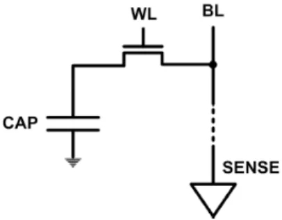
DRAM Subsystem Organization
DRAM Subsystem Organization A DRAM bank is a 2D array of cells: rows x columns
A “DRAM row” is also called a “DRAM page”
“Sense amplifiers” also called “row buffer”
Each address is a {row,column} pair
Access to a “closed row”
Activate command opens row (placed into row buffer)
Read/write command reads/writes column in the row buffer
Precharge command closes the row and prepares the bank for next access
Access to an “open row”
No need for an activate command
DRAM Bank Operation
注: 一个 bank 就是一个二维阵列. 如果数据不在 buffer 内, 需要通过 Row decoder 选择行, 破坏性读(DRAM)到 Row Buffer 中. 通过列译码得到需要的 Data 把数据传出.
Consists of multiple banks (8 is a common number today)
Banks share command/address/data buses
The chip itself has a narrow interface (4-16 bits per read)
Changing the number of banks, size of the interface (pins), whether or not command/address/data buses are shared has significant impact on DRAM system cost
128M x 8-bit DRAM Chip
DRAM Rank and Module
Rank: Multiple chips operated together to form a wide interface
All chips comprising a rank are controlled at the same time
Respond to a single command
Share address and command buses, but provide different data
A DRAM module consists of one or more ranks
E.g., DIMM (dual inline memory module)
This is what you plug into your motherboard
A 64-bit Wide DIMM (One Rank)
Advantages:
Acts like a high-capacity DRAM chip with a wide interface
Flexibility: memory controller does not need to deal with individual chips
Disadvantages:
Granularity: Accesses cannot be smaller than the interface width
Generalized Memory Structure
The DRAM subsystem
Breaking down a DIMM
Rank
Breaking down a Rank
Example: Transferring a cache block
Transferring a cache block Transferring a cache block Transferring a cache block 


